Most people know two kinds of magnetism: the kind that sticks a note to a fridge, and the kind that hides inside some materials and produces no outside field at all. Physicists now have a candidate for a third, and a team at the University of Central Florida says it has found experimental evidence of it in a thin, layered crystal.
The material is Co₁/₄TaSe₂, which contains magnetic cobalt atoms. The team, led by physics professor Madhab Neupane, reports signatures of altermagnetism, according to a university release carried by ScienceDaily and a report on Phys.org.
What altermagnetism is
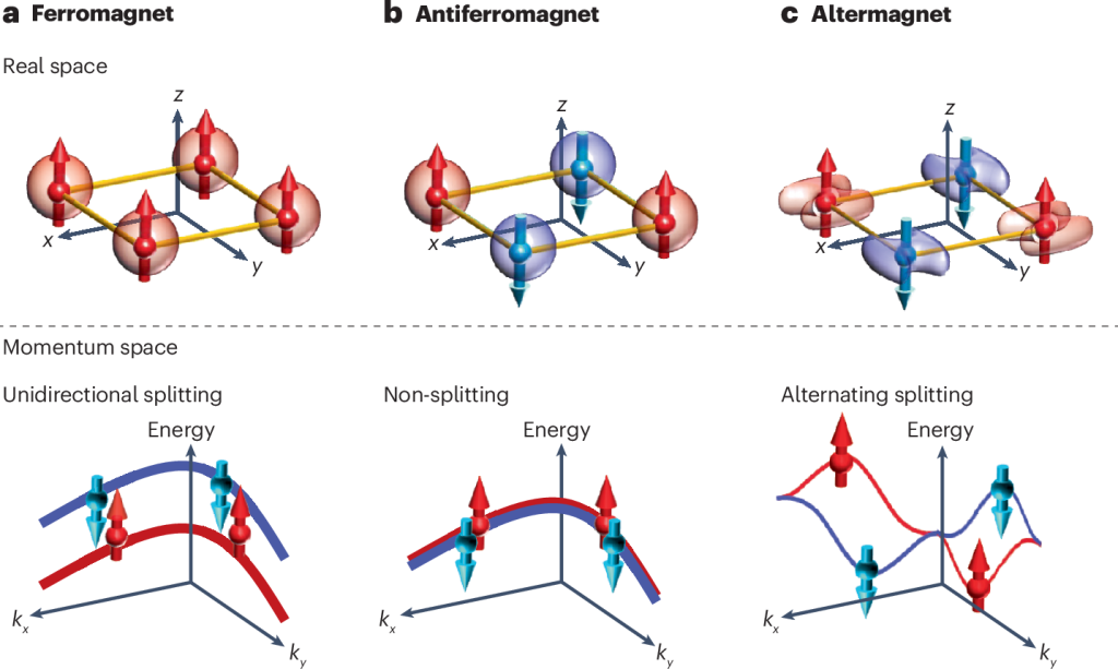
Altermagnetism is a recently described magnetic state. As ScienceAlert explains, it combines useful traits of two familiar types.
Ferromagnets, such as ordinary bar magnets, are good at separating electrons by spin because their magnetic moments line up. But they produce stray magnetic fields. Antiferromagnets have moments that point in opposite directions and cancel out, so they leave no stray field. They are poor at separating spins.
An altermagnet is meant to offer the clean, field-free behavior of an antiferromagnet while still splitting electrons by spin, as a ferromagnet does.
Why electronics makers care
Today’s chips mostly rely on electrical charge. Spintronics aims to use the electron’s spin as well, which researchers hope could lead to faster, thinner and more energy-efficient devices. Stray magnetic fields are a nuisance there, because they can interfere with neighboring components. A material without them would help.
The release says the unusual magnetic state may allow such devices without the interference caused by conventional magnets. That is a possibility, not a demonstrated product.
How the team looked for it
The researchers used photoemission, a technique that measures the energy levels of electrons in a material’s surface. Samples were checked for exceptionally clean surfaces before measurement. Work was done at national facilities, including the Advanced Light Source at Lawrence Berkeley National Laboratory and the Stanford Synchrotron Radiation Lightsource, according to Phys.org.
First, they used high-resolution methods that do not depend on spin and found a characteristic splitting in the electronic bands. Then they used spin-resolved photoemission to look closer. The split states carried opposite spin polarizations, which is key evidence for altermagnetism.
Neupane said confidence grew once the measurements consistently matched theoretical predictions. In the university’s account, the team concluded it had identified a genuine layered altermagnet.
A material that can be modified
The crystal’s structure is part of the appeal. It is made of extremely thin sheets stacked together, and the layers are only weakly connected. Researchers can therefore separate them and combine them into very thin structures, which suits thin-film devices.
Milo Sprague, the study’s lead graduate student, said that evidence of altermagnetism in a versatile platform opens up many new possibilities. He also pointed to an open argument in the field: theorists still debate how spin-polarized electronic states interact with other magnetic phenomena. A material that is easy to modify gives experimenters a way to test those questions.
What remains unproven
The reports describe evidence of altermagnetic order, not a working device. Other groups have been exploring the same idea in different materials. The Advanced Light Source has described separate work on chromium antimonide thin films, where altermagnetic band splitting was seen in samples relevant to real devices.
Questions such as how stable the effect is, how well it works at practical temperatures, and how the layers could be built into circuits are not answered in the coverage reviewed. For now, the result adds a flexible test bed to a young field, and independent confirmation will matter.